Introduction
When I designed the main board of the Nestronic, I was busy enough that I didn't want to hold up progress on account of other areas of the project. I basically just figured out what interface pins I might need for an input board, brought them out to a connector, and set that part aside.
I figured I'd need an I2C bus to interface with some sort of I/O expansion chip, and a few support
GPIO pins. I also thought it might be neat to try experimenting with the ESP32's
touch sensor capabilities, so I made sure at least one of the GPIO pins could be used for that.
(For more project background, please read the [
Introduction], [
Architecture], and [
Prototype Assembly] blog posts.)
Selecting Components
One idea I had for using a capacitive touch sensor would be as a way of implementing an alarm clock "snooze button" on the top of the enclosure. After all, if the Nestronic is going to be capable of acting as an alarm clock, it should probably have this.
To implement such a touch button, I'd need some sort of conductive surface that could be built into the enclosure and wired up to the input board. As I explored the new world of 3D printing, I discovered
Proto-pasta's
Conductive PLA filament and made a few test prints. The idea was to combine this with the dual-extrusion capabilities of my 3D printer, and embed a conductive area into the project enclosure.
In tests, the material was sometimes be a bit messy, but it worked! To connect wires to it, I used a metal screw on the bottom.
 |
| Capacitive Touch Test Prints |
The next step was to select the push buttons for the rest of the input board. After searching in the usual places, I found a line-up of simple tactile switches that were designed for key-caps to sit on top. I ordered these switches in a few varieties with different press forces, tested them out, and decided on one to use.
 |
| Tactile Switch Options |
To mimic the layout of a NES controller, I knew I would need about eight buttons. To manage this, I'd need some sort of I/O expansion or keypad controller IC. After doing a lot of research, I eventually settled on the
TCA8418 Keypad Scan IC.
For initial testing, I soldered this IC onto a breakout board and combined it with a bunch of
breadboard-friendly tactile switches. Everything seemed to work great, so I moved on to actually doing a circuit schematic and PCB design.
 |
| Input Buttons on Breadboard |
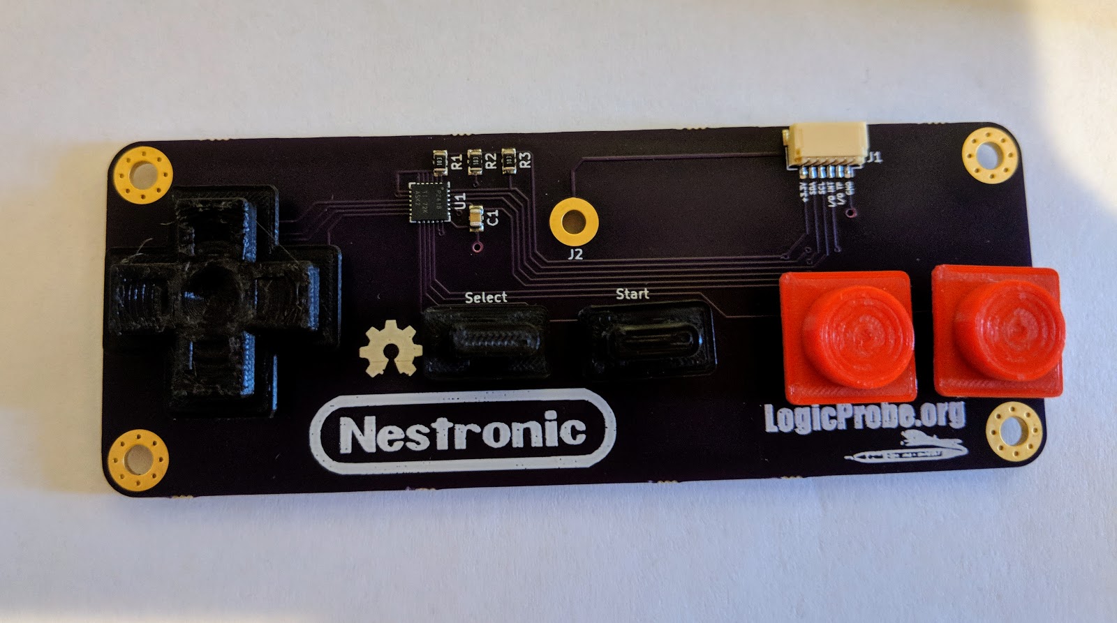
Designing the Board
The actual design of the board was rather simple. I connected the TCA8418 to 8 switches in a non-matrix mode, added necessary pull-up resistors, and made sure I had connectors in the right places.
 |
| Input Board Schematic |
The PCB layout took a little bit more work, since the most important part of this design was the physical position of the switches. To figure this out, measured an actual NES controller and translated the numbers into something relative to KiCad switch footprints. I also had to take the mounting location of the board into account, which meant using a right-angle connector for the cable and putting some silkscreen markings on the bottom.
 |
| Input Board PCB Layout |
Once everything looked good, I went ahead and placed all the orders. This was the usual routine of PCBs from
OSH Park, a stencil from
OSH Stencils, and any additional components from
Digi-Key.
Assembling the Board
A few weeks later, I was ready to begin!
 |
| Input PCB Ready for Assembly |
Getting the PCB ready for components
 |
| PCB Taped Down in Jig |
|
 |
| Stencil in Position |
|
 |
| Paste Spread Across |
|
 |
| Stencil Removed |
|
Assembling the Board
 |
| Ready for Component Placement |
 |
| Microscope Close-Up |
|
 |
| 0805 Components (Some say these are "big") |
|
 |
| Surface Mount Components Placed |
|
 |
| Reflow Soldering |
|
 |
| Reflow Complete |
|
 |
| Thru-hole Components Placed |
|
Final Assembly
The last step was to make key caps for all the buttons and then install the board into the enclosure. This was done using careful measurements, 3D printing, and some trial-and-error. Thankfully the key caps print quickly, so iterating wasn't too painful.
 |
| 3D Printed Key Caps |
Once I installed everything into the enclosure, things wrapped up quite nicely. The buttons had a little jiggle, which is hard to avoid at 3D printer tolerances, but overall I'm quite pleased with the results.
 |
| Installed in Enclosure |
Conclusion
This post wraps up everything I plan to write about Revision A of the Nestronic. There may be more posts, covering Revision B (currently a work-in-progress) and the software (which continues to evolve).
Thus far I've mostly focused on the design and assembly of the electronics in this project. That is actually only one piece of this project. Plenty of additional work has also gone into the software (C and 6502 assembly) and the enclosure (CAD work and 3D printing).
For revision B, the only change to this module will be the addition of an ambient light sensor (due to issues with the main-board one I originally planned to use) and some tweaks to the 3D printed enclosure model. Otherwise, everything has been working perfectly.
Going forward, I'm now keeping all the design materials for this project public. They're available in a
Git repository, and will be regularly updated as work progresses.


No comments:
Post a Comment